Diferencia entre polarización directa e inversa con cuadro comparativo Zener diode reverse bias circuit diagram Pn junction diode and diode characteristics
Electrical – Voltage across Zener diode – Valuable Tech Notes
Electrical – voltage across zener diode – valuable tech notes Schematic diagram of forward biased diode Reverse bias circuit diagram
Schematic diagram of forward biased diode
Diodes and diode circuitsReverse biasing of pn junction diode Reverse forward circuit biasing diode junction bias distinguish diagrams between sarthaks help characteristics iiDiode bias rectifier.
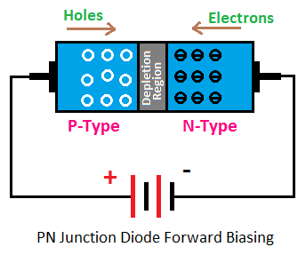
☑ diode zero biasDiode forward bias circuit diagram What is forward bias and reverse bias? example, applicationsView zener diode forward and reverse bias circuit diagram.

Electronic – voltage drop – diode reverse biased – valuable tech notes
Forward biasing of pn junction diodeCircuit diagram of zener diode in forward bias Semiconductor diode forward bias☑ diode zero bias.
Junction forward bias curve characteristic diode biasedDiode pn semiconductor junction reverse bias depletion layer working characteristics circuit notes flow current region physics electronics choose board connection Semiconductor pn junction diode workingReverse diagram bias diode biased.

Diode in forward and reverse bias
Forward biased circuit diagramMiirbe pn junction diode reverse bias circuit diagram Diode junction pn forward bias characteristics circuit biasing reverse ammeter voltmeter plot sourcePn junction diode and its forward bias & reverse bias characteristics.
To draw the i-v characteristic curve of a p-n junction in forward bias51+ which of the following appear in the diagram below P n junction diode,Get 42 zener diode reverse bias circuit diagram.

How does a diode work? (part 3
Reverse bias diode circuit diagramReverse biasing of pn junction diode Diode junction pn biasing bias electricalworkbook biased definitionSemiconductor diode.
Pin by sathathini sivam on electrical engineering articlesBias biasing pn diode junction etechnog transistors barrier Rectifier diode : circuit diagram, biasing and its applications(i) with the help of circuit diagrams distinguish between forward.

Diode junction pn characteristics bias semiconductor barrier gif battery
Diode bias calculation figureDiode circuits diodes reverse biased bias practical affect electronics drop Forward bias, reverse bias and their effects on diodes.
.

What is Forward Bias and Reverse Bias? Example, Applications - ETechnoG

P N Junction diode, - STUDYTRONICS

(i) With the help of circuit diagrams distinguish between forward

51+ which of the following appear in the diagram below - DauneVinessa

Electrical – Voltage across Zener diode – Valuable Tech Notes

Get 42 Zener Diode Reverse Bias Circuit Diagram | Images and Photos finder

Electronic – Voltage drop – Diode reverse biased – Valuable Tech Notes